Guide
KiCad project generator does not generate PCBs ready for fabrication. User needs to design microcontroller circuit and route everything together.
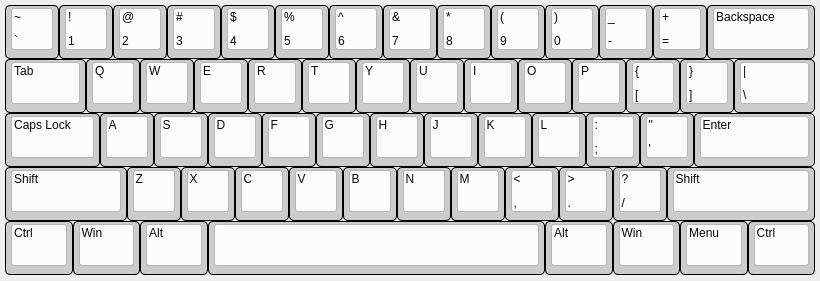
In this guide I'm using Default 60% preset from keyboard-layout-editor.
Recommended workflow contains following steps:
Download json layout of your design (attention: this is not data from Raw data tab. Use Download JSON button).
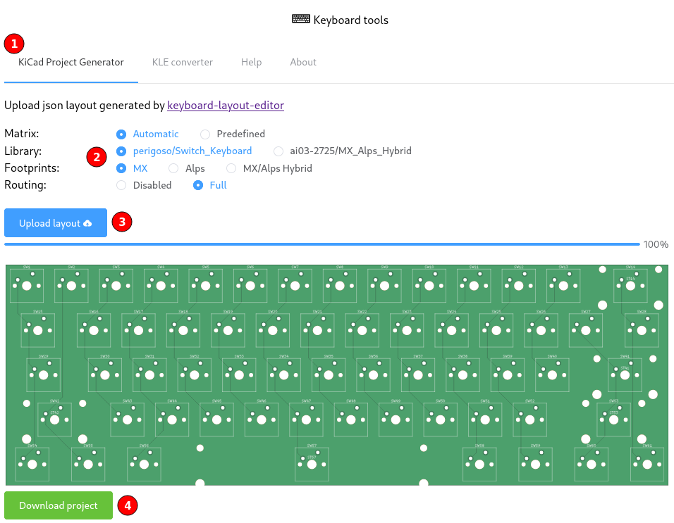
Go to keyboard-tools's KiCad Project Generator tab (1), choose project options (2) and upload keyboard layout (3).
In this example I decided to use Cherry MX footprints and I enabled routing. Because I did not used key annotations (see this) I used Automatic matrix option.
If everything succeed, after few seconds, PCB preview and Download project button (4) should appear:
Download and unzip project. Open project located in
keyboarddirectory. It should contain following structure: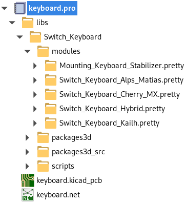
TIP
Generated project has entire selected switch library bundled in. This makes footprint replacement easy.
keyboard.kicad_pcbfile should have switches and diodes placed according to provided layout like this: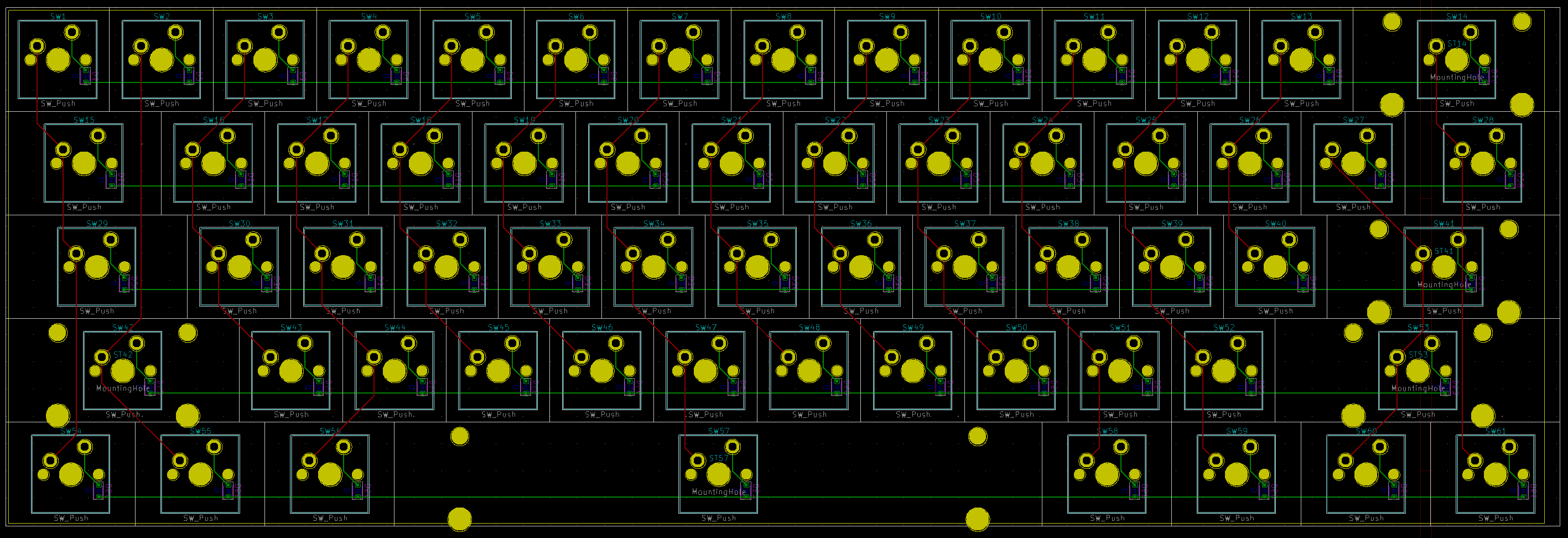
Run DRC check. In this example, there is one invalid track.
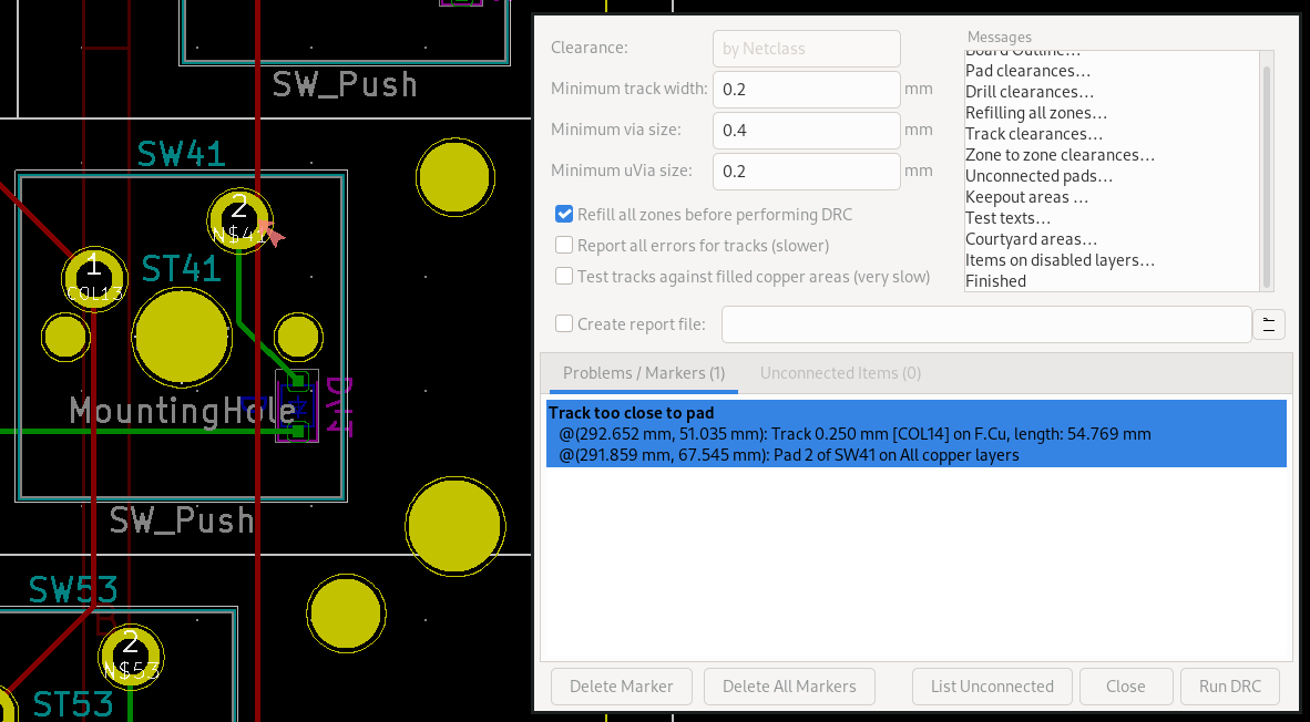
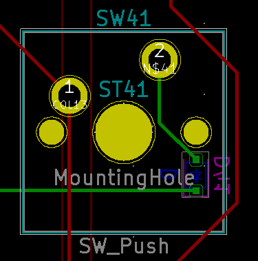
In order to fix it, simple remove faulty track segment and route it manually, for example:
Also check if DRC report any unconnected items. For some layouts, current router implementation does not attempt to connect items (mainly diodes with different
Ycoordinate).TIP
Always run DRC check on imported projects. Implemented router does not guarantee that rules are met, for details see this.
From this point onward, PCB needs to be finished by user.
Open
Schematic Layout Editor, because schematic is not generated there will be following prompt: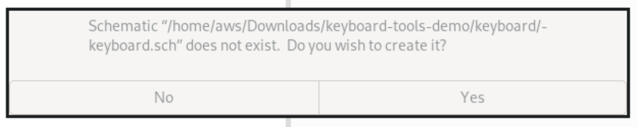
Select yes.
Design microcontroller circuit, for example:
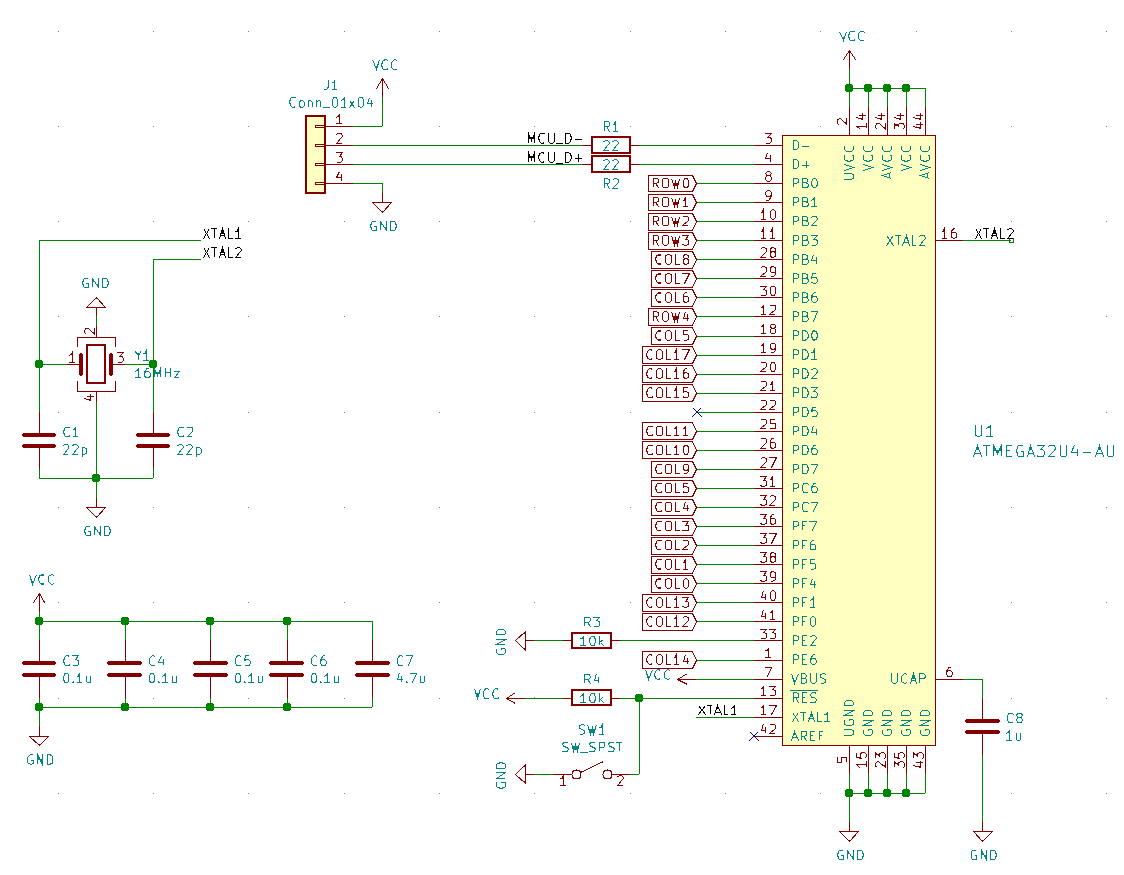
For connecting key matix rows/collumns use
Global Labelswith following name convention:ROW{number}/COL{number}TIP
Generating MCU circuitry is planned in future releases.
Generate netlist (
Tools->Generate Netlist File). Remember to rename it, otherwise key matrix netlist will be overwritten (by default, KiCad names netlist same as project).Open
keyboard.kicad_pcband load microcontroller netlist.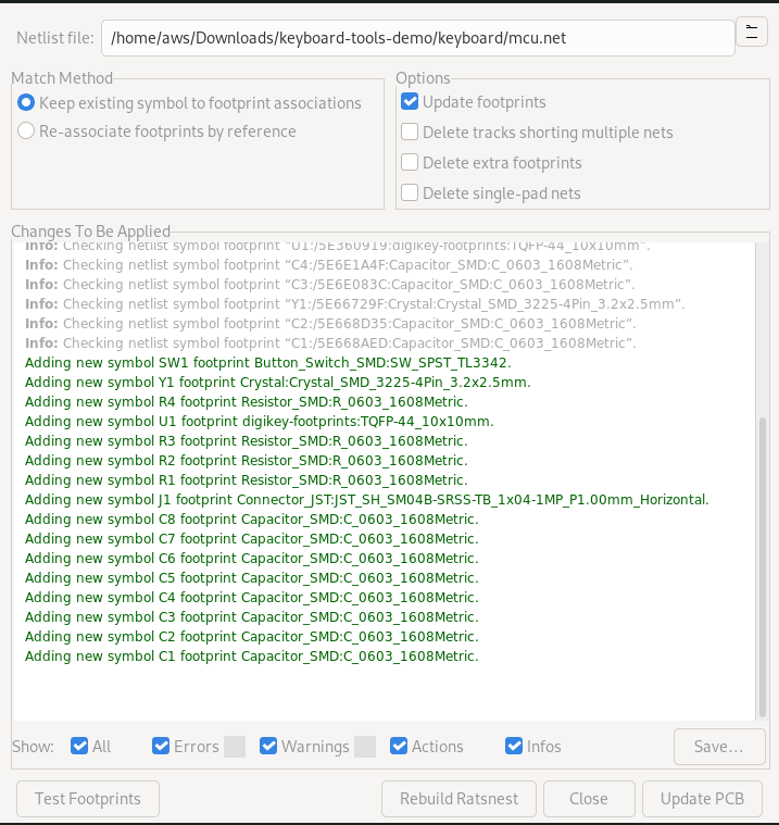
Click Upadate PCB and Close. New components will appear on PCB.
Finish placement and routing.